- 您现在的位置:买卖IC网 > Sheet目录472 > MAX2121EVKIT# (Maxim Integrated)KIT EVAL FOR MAX2121
�� �
�
�Complete� Direct-Conversion� L-Band� Tuner�
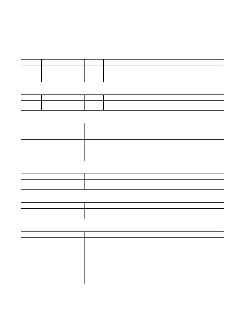
�Table� 2.� N-Divider� MSB� Register� (Address:� 0x00)�
�BIT� NAME�
�FRAC�
�N[14:8]�
�BIT� LOCATION� (0� =� LSB)�
�7�
�6� –0�
�DEFAULT�
�1�
�0000000�
�FUNCTION�
�Users� must� program� to� 1� upon� powering� up� the� device.�
�Sets� the� most� significant� bits� of� the� PLL� integer-divide� number� (N).� N� can�
�range� from� 19� to� 251.�
�Table� 3.� N-Divider� LSB� Register� (Address:� 0x01)�
�BIT� NAME�
�N[7:0]�
�BIT� LOCATION� (0� =� LSB)�
�7� –0�
�DEFAULT�
�00100011�
�FUNCTION�
�Sets� the� least� significant� bits� of� the� PLL� integer-divide� number.� N� can� range�
�from� 19� to� 251.�
�Table� 4.� Charge-Pump� Register� (Address:� 0x02)�
�BIT� NAME�
�CPMP[1:0]�
�CPLIN[1:0]�
�F[19:16]�
�BIT� LOCATION� (0� =� LSB)�
�7� –6�
�5� –4�
�3� –0�
�DEFAULT�
�00�
�00�
�0010�
�FUNCTION�
�Charge-pump� minimum� pulse� width.� Users� must� program� to� 00� upon�
�powering� up� the� device.�
�Controls� charge-pump� linearity.� Users� must� program� to� 01� upon� powering�
�up� the� device.�
�Sets� the� 4� most� significant� bits� of� the� PLL� fractional� divide� number.�
�Default� value� is� F� =� 194,180� decimal.�
�Table� 5.� F-Divider� MSB� Register� (Address:� 0x03)�
�BIT� NAME�
�F[15:8]�
�BIT� LOCATION� (0� =� LSB)�
�7� –0�
�DEFAULT�
�11110110�
�FUNCTION�
�Sets� the� most� significant� bits� of� the� PLL� fractional-divide� number� (F).�
�Default� value� is� F� =� 194,180� decimal.�
�Table� 6.� F-Divider� LSB� Register� (Address:� 0x04)�
�BIT� NAME�
�F[7:0]�
�BIT� LOCATION� (0� =� LSB)�
�7� –0�
�DEFAULT�
�10000100�
�FUNCTION�
�Sets� the� least� significant� bits� of� the� PLL� fractional-divide� number� (F).�
�Default� value� is� F� =� 194,180� decimal.�
�Table� 7.� XTAL� Buffer� and� Reference� Divider� Register� (Address:� 0x05)�
�BIT� NAME�
�BIT� LOCATION� (0� =� LSB)�
�DEFAULT�
�FUNCTION�
�Sets� the� crystal-divider� setting.�
�000� =� Divide� by� 1.�
�001� =� Divide� by� 2.�
�XD[2:0]�
�7� –5�
�000�
�011� =� Divide� by� 3.�
�100� =� Divide� by� 4.�
�101� through� 110� =� All� divide� values� from� 5� (101)� to� 7� (110).�
�111� =� Divide� by� 8.�
�Sets� the� PLL� reference-divider� (R)� number.� Users� must� program� to� 00001�
�R[4:0]�
�4� –0�
�00001�
�upon� powering� up� the� device.�
�00001� =� Divide� by� 1;� other� values� are� not� tested.�
�11�
�发布紧急采购,3分钟左右您将得到回复。
相关PDF资料
MAX2130EVKIT
EVAL KIT MAX2130
MAX2140EVKIT
EVAL KIT MAX2140
MAX2150ETI+T
IC MODULATOR I/Q WIDE 28TQFN
MAX2160EVKIT
EVAL KIT MAX2160
MAX2163ETI/V+
IC TUNER ISDB-T LOW IF 28TQFN
MAX2165EVKIT+
KIT EVAL FOR MAX2165
MAX2170EVKIT+
KIT EVAL FOR MAX2170
MAX2202EWT+T
IC POWER DETECTOR RMS 6-WLP
相关代理商/技术参数
MAX212C/D
功能描述:RS-232接口集成电路 +3V Powered Low-Power True RS-232 Transceiver RoHS:否 制造商:Exar 数据速率:52 Mbps 工作电源电压:5 V 电源电流:300 mA 工作温度范围:- 40 C to + 85 C 安装风格:SMD/SMT 封装 / 箱体:LQFP-100 封装:
MAX212CAG
功能描述:RS-232接口集成电路 RoHS:否 制造商:Exar 数据速率:52 Mbps 工作电源电压:5 V 电源电流:300 mA 工作温度范围:- 40 C to + 85 C 安装风格:SMD/SMT 封装 / 箱体:LQFP-100 封装:
MAX212CAG+
功能描述:RS-232接口集成电路 3V True RS-232 Transceiver RoHS:否 制造商:Exar 数据速率:52 Mbps 工作电源电压:5 V 电源电流:300 mA 工作温度范围:- 40 C to + 85 C 安装风格:SMD/SMT 封装 / 箱体:LQFP-100 封装:
MAX212CAG+T
功能描述:RS-232接口集成电路 3V True RS-232 Transceiver RoHS:否 制造商:Exar 数据速率:52 Mbps 工作电源电压:5 V 电源电流:300 mA 工作温度范围:- 40 C to + 85 C 安装风格:SMD/SMT 封装 / 箱体:LQFP-100 封装:
MAX212CAG-T
功能描述:RS-232接口集成电路 RoHS:否 制造商:Exar 数据速率:52 Mbps 工作电源电压:5 V 电源电流:300 mA 工作温度范围:- 40 C to + 85 C 安装风格:SMD/SMT 封装 / 箱体:LQFP-100 封装:
MAX212CWG
功能描述:RS-232接口集成电路 RoHS:否 制造商:Exar 数据速率:52 Mbps 工作电源电压:5 V 电源电流:300 mA 工作温度范围:- 40 C to + 85 C 安装风格:SMD/SMT 封装 / 箱体:LQFP-100 封装:
MAX212CWG-T
功能描述:RS-232接口集成电路 RoHS:否 制造商:Exar 数据速率:52 Mbps 工作电源电压:5 V 电源电流:300 mA 工作温度范围:- 40 C to + 85 C 安装风格:SMD/SMT 封装 / 箱体:LQFP-100 封装:
MAX212EAG
功能描述:RS-232接口集成电路 RoHS:否 制造商:Exar 数据速率:52 Mbps 工作电源电压:5 V 电源电流:300 mA 工作温度范围:- 40 C to + 85 C 安装风格:SMD/SMT 封装 / 箱体:LQFP-100 封装: